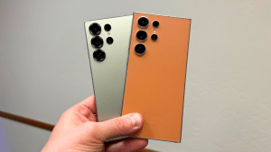
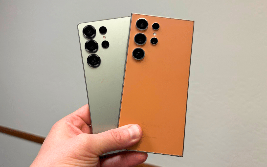
Samsung Bets $770 Million on High-NA EUV to Boost Semiconductor Leadership

SammyGuru is reader-supported. We have affiliate and sponsored partnerships, so we may earn a commission when you buy through links on our site — at no extra cost to you. Learn more.
Samsung is making a major push to strengthen its semiconductor business, signaling renewed confidence in both its foundry and memory operations. The company plans to invest around $770 million over the next few months to introduce two units of the latest High-NA EUV lithography equipment from Dutch supplier ASML. The new EUV systems are capable of printing circuits 1.7 times finer than current models.
Samsung to buy advanced EUV lithography equipment for its foundry
According to the Korean media, Samsung will bring in one High-NA EUV machine by the end of this year and add the second unit in the first half of 2026. Each unit costs around 550 billion KRW (approx. $385 million), making it the most expensive semiconductor manufacturing tool available. The company had previously installed a High-NA EUV system at its Hwaseong campus for R&D purposes only.
The new system increases the numerical aperture (NA) from 0.33 to 0.55, a 40% improvement, enabling finer patterning resolution and paving the way for more advanced chips. “Samsung is making a bet to improve the technology of the next-generation process,” an industry insider said. The investment reflects the company’s focus on staying ahead in the next era of semiconductor manufacturing.
Samsung’s semiconductor business has been showing clear signs of revival. Exynos chips have steadily improved in performance, reflecting advances in Samsung’s foundry capabilities. Meanwhile, memory sales remain strong, with DRAM and NAND demand holding up despite global market fluctuations. There are also early indications that Samsung may have finally cracked the HBM market.
HBM chips are critical for AI, high-performance computing, and next-generation graphics applications. Success in this space would further solidify Samsung’s leadership in the semiconductor industry. It missed the early boom, but with Nvidia’s approval seemingly done, the Korean giant is well-positioned to tap the market soon. The latest High-NA EUV lithography equipment may give it a technological edge against rivals.
Written by
Sumit AdhikariSumit, a life-long Samsung user, is passionate about technology and has been professionally writing on tech since 2017. He’s a mathematics graduate by education and enjoys teaching basic mathematics tricks to school kids in his spare time. Sumit believes in artificial intelligence and dreams of a fully open, intelligent and connected world.
Follow us on Google Discover & set us as a preferred source in Google News
Share this Post
___________________________


New Blog Posts
___________________________
First Set of Pixel 11 Pro XL Renders Are Here
Pixel 11 Pro XL CAD renders show minimal design changes

Is Samsung Preparing One UI 8.5 Beta for Galaxy Z Fold 5 and Flip 5?
Samsung may launch a One UI 8.5 beta program for its 2023 foldables
Galaxy S25 One UI 8.5 Beta May Run Longer Than Expected
Galaxy S25 series’ One UI 8.5 beta may stretch to 10 rounds